

China debuts integrated six-inch wafer polishing tool to boost EV chips
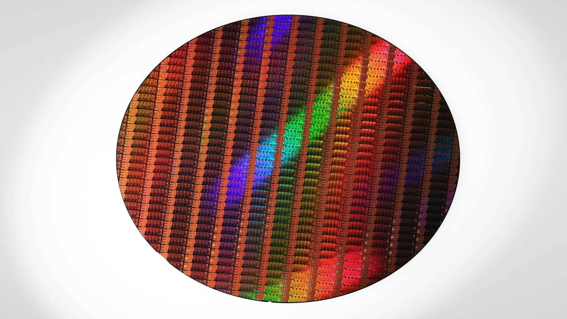
China-based Hwatsing Technology has taken a significant step forward in electronics manufacturing by advancing wafer polishing, aiming to reduce reliance on foreign supply chains.
Chinese chip developers continue to enhance their technical capabilities, achieving a new breakthrough in wafer polishing.
Wafer polishing, also known as chemical mechanical planarization (CMP), is a manufacturing process that uses chemical reactions and mechanical abrasion to make semiconductor silicon discs ultra-smooth and flat.
Manufacturers print, etch, and construct thousands of microscopic integrated circuits and transistors onto a single wafer before slicing it into individual microchips. The wafer serves as the base, or substrate, for producing integrated circuits, microchips, and other microdevices.
As China’s top producer of semiconductor production equipment, Hwatsing Technology announced a new metrology system paired with chemical mechanical polishing equipment for six-inch wafers – a first for the country.
A critical step in electronics manufacturing has made measurable progress
On Thursday, the partially state-owned Chinese company Hwatsing Technology announced an innovation in semiconductor manufacturing.
The industry still depends on foreign suppliers for these complex processes. As the South China Morning Post notes, turning “a raw wafer into a finished chip requires multiple steps, including coating the surface with photoresist, etching intricate layers, and wiring microscopic transistors.”
In practice, wafers must move between separate polishing machines and inspection systems, which slows down production.
The company’s new six-inch metrology system provides real-time measurements before and after polishing. It transmits live data to the control system to enable defect detection and ensure consistent output quality.
With this integrated innovation, the company aims to improve wafer uniformity and reduce waste, addressing key production challenges. Because even a microscopic impurity can ruin an entire batch of chips, the manufacturing environment must be cleaner than an operating room.
The company intends to target chips used in “power devices, microelectromechanical systems and sensors, mostly with mature processing nodes. Such devices are widely used in electric vehicles, industrial equipment, consumer electronics and telecommunications infrastructure,” according to the South China Morning Post.
Could this development shift the global market in China’s favor?
Verified Market Research describes the Silicon Wafers Market as a specialized, high-technology industry that supplies the essential “blank canvas” for the digital world.
The South China Morning Post referenced the “advanced bottlenecks” that typically capture the world’s attention, such as EUV, or Extreme Ultraviolet lithography. ASML, a Dutch company, has a 100% global monopoly on manufacturing these machines.
However, domestic companies such as Hwatsing are developing solutions for semiconductor processes like etching, chemical mechanical planarization (CMP), wafer polishing, and nascent immersion DUV systems.
Some believe this could shift the global market, while others argue that “progress remains constrained in lithography,” a field dominated by ASML, which is currently barred from selling its most advanced systems to China.
While these improvements enhance factory systems and reduce waste, wafers are just one piece of the geopolitical puzzle. As Santiago and Company concluded, “the primary bottleneck has shifted from wafer fabrication to physical integration.”
Though Hwatsing remains the “undisputed leader,” according to the South China Morning Post, “the self-sufficiency rate for wafer metrology and inspection tools” doesn’t quite measure up—not yet, at least.