Last week, Taiwanese manufacturer TSMC introduced the world’s most advanced microchip: the 2 nanometre chip. Mass production is expected for the second half of the year, and TSMC promises it will represent a major step forward in performance and efficiency – potentially reshaping the technological landscape.
Microchips are the foundation of modern technology, found in nearly all electronic devices, from electric toothbrushes and smartphones to laptops and household appliances. They are made by layering and etching materials like silicon to create microscopic circuits containing billions of transistors.
These transistors are effectively tiny switches, managing the flow of electricity and allowing computers to work. In general, the more transistors a chip contains, the faster and more powerful it becomes.
The microchip industry consistently endeavours to pack more transistors into a smaller area, leading to faster, more powerful and energy efficient devices.
Compared to the previous most advanced chip, which use a 3nm process, TSMC’s 2nm technology should deliver notable benefits. These include a 10-15% boost in computing speed at the same power level or a 20-30% reduction in power usage at the same speed.
Additionally, transistor density in 2nm chips is increased by about 15%, over and above the 3nm technology. This should enable devices to operate faster, consume less energy and manage more complex tasks efficiently.
Taiwan’s microchip industry is closely tied into its security. It is sometimes referred to as the “silicon shield”, because its widespread economic importance incentivises the US and allies to defend Taiwan against the possibility of Chinese invasion.
Foundry services
TSMC recently struck a US$100-billion deal to build five new US factories. However, there is uncertainty over whether the 2nm chips can be manufactured outside Taiwan, as some officials are concerned that could undermine the island’s security.
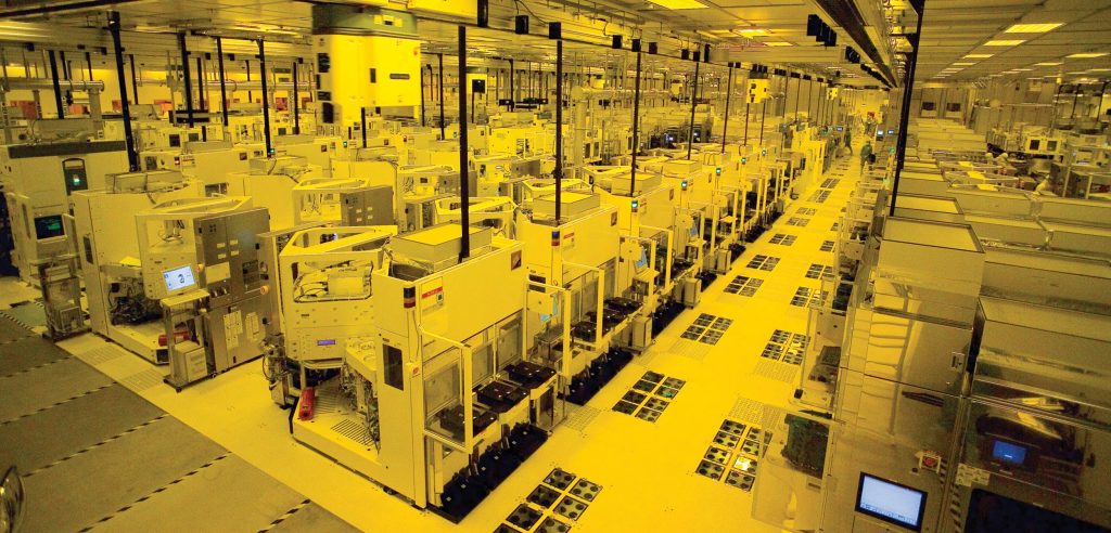
Established in 1987, TSMC, which stands for Taiwan Semiconductor Manufacturing Company, manufactures chips for other companies. Taiwan accounts for 60% of the global “foundry” market (the outsourcing of semiconductor manufacturing) and the vast majority of that comes from TSMC alone.
TSMC’s super-advanced microchips are used by other companies in a wide range of devices. It manufactures Apple’s A-series processors used in iPhones, it produces Nvidia’s graphics processing units used for machine learning and AI applications. It also makes AMD’s Ryzen and Epyc processors, and it produces Qualcomm’s Snapdragon processors, used in Samsung, Xiaomi, OnePlus and Google phones.
Read: New Intel CEO plots overhaul of manufacturing and AI operations
In 2020, TSMC moved to 5nm FinFET technology that played a crucial role in smartphone and high-performance computing development.
Two years later, it launched a 3nm miniaturisation process based on even smaller microchips. This further enhanced performance and power efficiency. Apple’s current A-series processor, for example, is based on this technology.
Smartphones, laptops and tablets with 2nm chips could benefit from better performance and longer battery life. This will lead to smaller, lighter devices without sacrificing power.
The efficiency and speed of 2nm chips have the potential to enhance AI-based applications such as voice assistants, real-time language translation and autonomous computer systems (those designed to work with minimal to no human input). Data centres could experience reduced energy consumption and improved processing capabilities, contributing to environmental sustainability goals.
Autonomous vehicles and robotics could benefit from the increased processing speed and reliability of the new chips, making these technologies safer and more practical for widespread adoption.
This all sounds really promising, but while 2nm chips represent a technological milestone, they also pose challenges. The first one is related to the manufacturing complexity.
Producing 2nm chips requires cutting-edge techniques like extreme ultraviolet (EUV) lithography. This complex and expensive process increases production costs and demands extremely high precision.
Another big issue is heat. Even with relatively lower consumption, as transistors shrink and densities increase, managing heat dissipation becomes a critical challenge.
Overheating can impact chip performance and durability. In addition, at such a small scale, traditional materials like silicon may reach their performance limits, requiring the exploration of different materials.
New era
That said, the enhanced computational power, energy efficiency and miniaturisation enabled by these chips could be a gateway to a new era of consumer and industrial computing. Smaller chips could lead to breakthroughs in tomorrow’s technology, creating devices that are not only powerful but also discreet and more environmentally friendly.![]()
- The author, Domenico Vicinanza, is associate professor of intelligent systems and data science, Anglia Ruskin University
- This article is republished from The Conversation under a Creative Commons licence. Read the original article
Don’t miss:
New Intel CEO tells clients: ‘Be brutally honest with us’
Crédito: Link de origem


